
Almost all of the technology we use today is based on the microprocessor. There can be few electrical devices, really only the most basic, whose capabilities are not now defined by software running on a microprocessor chip within. Those chips’ designs are different, and some incorporate much more ancillary functionality than others, but their fundamental architecture is the same: a set of logic and arithmetical units operated in a predetermined sequence by a set of program instructions. The result: a general purpose machine that can be changed to do almost anything — you just keep feeding it different programs. Car engine management; central heating control; TV interface; games console; washing machine cycle… you name it, they use the same chips, just run different code.

But how did the microprocessor itself emerge? This coming week marks the 50th birthday of the microprocessor, dated to the launch of the first commercially available model, the Intel 4004. It wasn’t sold individually, as a microprocessor, but as one of a suite of chips to be used as the basis of whatever device the customer was creating. Similar technology had already been developed for very specific roles, but in contexts — military and aerospace — that meant that they would have no wider impact, or even be made public at all until many, many years later. The 4004 wasn’t even the first microprocessor to be discussed in public — that honour goes to Texas Instruments. But it was the first to be realised as a working product that any electronics engineer could use. This is the story of how it came about, and that of its near twin, the 8008. Neither was a huge success, but the chips they inspired, not only from Intel but from many other semiconductor manufacturers, would be.
When the 4004 was launched, in November 1971, Intel’s advertising copywriters felt able to announce “a new era of integrated electronics”. Yet Intel firmly expected to continue making almost all of its money — and at the time it was making plenty — from selling memory chips, the products it had been founded in 1968 to make. However, it was a statement that would quickly prove to be prophetic.
The 4004 was developed by a small team led by a new Intel recruit, electronics engineer Federico Faggin, an Italian who had just joined the company from Fairchild, the firm from which Intel’s own founders had quit to establish their new venture less than two years previously. Faggin started work on the 4004, his first work for Intel, in April 1970. At this point the chip was already almost six months behind schedule. A year before, a Japanese calculator company, the Business Computer Corporation – Busicom, for short — asked Intel to design a set of chips for a large, sophisticated but low-cost desktop calculator it was planning to bring to market. In some ways it was an unusual request to make of a memory specialist like Intel, which at that point had no experience in designing this kind of custom chip. But Intel was young and hungry, and Busicom figured it would be willing to work on the project because it wasn’t in a position to turn work away. More to the point, Intel would do the work for less money than its better established competitors were expected to demand.
Enter Busicom
The head of Intel’s Applications Research Department, Marcian E Hoff — ‘Ted’ to his colleagues; his middle name is Edward — considered the Busicom request in light of the limited resources Intel would be able to dedicate to the project. Hoff was an Intel original: he was the firm’s twelfth employee. His role was to explore the possible applications to which Intel’s products might be put, essentially sniffing out new markets for existing products. His department was the obvious place to route Busicom’s request for assistance when then Japanese firm knocked on Intel’s door in the Spring of 1969. The Busicom calculator specification called for eight separate custom chips, and in the discussions that followed the the Japanese company’s approach, Intel’s bosses weren’t sure they would be able to design and develop that many chips in the time allowed, especially since they would be starting from scratch. Like a modern day Alexander, Hoff quickly saw how he could cut right through the Busicom blueprint’s Gordian complexity. He’d been using a DEC minicomputer for circuit design work and general programming. He realised that even this physically imposing machine was architecturally less complicated than the proposed calculator. The minicomputer’s architecture could be envisaged as a combination of a handful of functional elements: a processing unit, memory, storage, and input and output controllers — an architecture going back to the early days of electronic computing. Implement each one of those elements in the form of a chip, Hoff reasoned, and Intel would have a more simple alternative to the solution Busicom was seeking and yet one that, architecturally at least, would have all the capabilities of the general-purpose minicomputer. Rather than create components specific to Busicom’s design, surely it would be better to devise a compact computer and simply program it with a calculator application?
Hoff’s insight was important, but it wasn’t an entirely radical breakthrough. The evolution of the integrated circuit through the 1960s had been one of combining ever more once-discrete electronic components into increasingly capacious chips. Integrated circuits had started out containing just a few transistors, resistors, capacitors and such as a single circuit. Evolving IC technology allowed those original ICs to be combined into new chips containing a handful of circuits, and so on into ICs with hundreds and then thousands of circuits. Various companies, including Rockwell and Fairchild, had created bit-at-a-time serial CPUs on silicon. At that point, it wasn’t so much a question of whether anyone would produce a chip that contained all of the circuits you would find on a minicomputer’s CPU board but when.
In June 1969, a team of three Busicom engineers visited Intel to hand over their calculator design into which the Intel chips would be fitted. Hoff subsequently sketched out a general-purpose processor chip which would be accompanied by separate memory and program storage chips, plus a fourth to control the Busicom calculator’s keypad and display. Four chips in place of ten. Hoff’s proposed processor might be considerably more complex than any one of the ten chips Busicom had asked for, but the four-chip option would, he thought, be cheaper and easier for Intel to design and manufacture. And instead of parts that could only be used in one specific scientific calculator, the Intel design could be re-purposed for other roles and other devices simply by reprogramming it. Even better: it could be the foundation for future custom logic chips, allowing Intel to begin pitching to hardware companies.
Hoff fires it off
Hoff’s bosses concurred, and the engineer’s proposal became the company’s pitch to Busicom. It took some time, but the Japanese firm, though not initially convinced by Hoff’s logic, was eventually persuaded that the scheme was the way forward. In October 1969, Busicom agreed to proceed with Hoff’s plan. Hoff was joined by Intel applications engineer Stan Mazor, who he himself had recruited from Fairchild the month before to work on the project. Helping out was their Busicom engineering liaison, Masatoshi Shima.
“When I joined Ted,” said Mazor in 2006, “he had one other chip that was proposed, which was a timing chip. I raised the question, ‘Well, why is there a separate timing chip?’ And ultimately Ted thought about that, and integrated the timing logic inside the CPU.” The result: the CPU could be done in a single chip.

The trio proceeded to nail the specifics of the four-chip architecture, and to define the CPU component’s instruction set — the list of operations it would be able to perform and from which any program it ran would be assembled. For example, the Busicom design called for the calculator’s arithmetic to be performed using binary coded decimal (BCD) format in order to make it easier receive and present decimal values. Hoff figured that rather than build the CPU to work in BCD, it would be much, much more simple to have it work straightforwardly in binary and include a single instruction to covert any binary result into the same value expressed in BCD notation. Such decimal adjust instructions would become common among all early microprocessors.
“There were so many things like that, that fell into place in the instruction set that it just seemed to write itself, almost,” he said in 2006.
Mazor used the instruction set to write some sample code to show how the Busicom engineers might program the new chip to deliver the calculator’s proposed functionality. That included the keyboard, display and printer drivers — or at least enough of each of them to demonstrate the feasibility of Intel’s suggestion for the Busicom design.
All this work took a month or so, to October 1969. With the specifications set, and informal approval granted to Intel, Shima returned to Japan with the expectation that he would return the following Spring and sign off on a final design which delivered those specifications. But as soon as Shima had departed, Hoff’s attention moved to the other tasks he was working on. Development work on the calculator chips halted while legal teams from Intel and Busicom worked to draw up a formal business agreement. This contract was subsequently signed in February 1970.
Customer number two
What was Hoff and his fellow engineers working on in the meantime? Busicom wasn’t the only company that had asked Intel to develop a custom chip. The Computer Terminal Company (CTC) approached Intel in the Summer of ’69, three or four months after Busicom had done so, because it required a set of 8-bit shift-registers for a multi-chip circuit board it was designing as the basis for a new Video Display Unit (VDU). A VDU combined a cathode ray tube display with a keyboard and was used to interact with minicomputers and mainframes. As the point at which the computer ended, and human input began, they were also called ‘terminals’. Unique programmability, CTC decided, would give its proposed Datapoint 2200 terminal a competitive edge over rival products. Different makes of mainframe communicated with terminals in different ways; the 2200’s programmability would allow it to be easily re-configured for whichever mini or mainframe a given Datapoint customer was using. CTC’s plan was to build the 2200’s processor out of a hundred or so transistor-transistor logic (TTL) chips, among them the shift registers it had asked Intel to provide. However, in a December 1969 conversation with CTC Vice-President Vic Poor, Intel’s Stan Mazor offered a number of suggestions to improve the CTC design. One proposal was to scrap engineer the serial processing unit being designed by Poor and engineer Harry Pyle, and implement the programmable terminal with what was essentially the Busicom architecture, which had just been completed by Hoff, Mazor and Shima. In short, abandon the 100-chip design for one based on a handul of chips that could also be programmed to deliver a terminal capable to working with any host machine. At this point, Intel wasn’t in a position to sell CTC the chips it had designed for Busicom, but it could sell the concept.
“I asked [Poor] about his computer and how smart it was, and what it had to do,” recalled Mazor in 2006. “I wrote out in front of him three proposals. One was an 8-bit register set with a stack, and another was a register stack with an arithmetic unit. And then I went on to the third proposal and said, ‘Well, it’s possible we could do the entire 8-bit CPU on one chip.’ Well, he certainly wasn’t about to believe that, but he was interested. I said, ‘But we need to know more about your computer before we could proceed with that.’ So in the January/February [1970] timeframe, he sent us an assembler language manual disclosing the instruction set of his computer.”
Mazor and Hoff together sketched out a rough specification for the CTC CPU, working to the instruction set and functionality CTC had already defined, though making some small changes in order to simplify the proposed chip’s eventual design. “Ted realized that they were sorely missing an increment and decrement instruction, so that was added,“ said Mazor. The CTC preliminary design called for a serial machine that would process multi-bit values one bit at a time. That was revised into a word-at-time parallel machine as per the 4004. In March 1970, Intel submitted a proposal to CTC based on Hoff and Mazor’s work. Intel suggested it should design an 8-bit CPU, codenamed the 1201, that could be incorporated into the Datapoint 2200. CTC liked the idea, and though Intel had not yet signed a formal contract with CTC, the chip company felt sufficiently confident to the hand the concept over to newly hired engineer Hal Feeney to be worked up into a full design. It was sure it had CTC in the bag.
New arrivals at Intel
That’s the situation Federico Faggin found when he arrived at Intel in April 1970. Intel’s Les Vasdasz, head of the MOS design group, was responsible for staffing the chip layout work and was responsible for bringing Faggin on board. Faggin had been preceded by Shima, who was making his anticipated return visit to the company to inspect the new chip. But where were the complete designs? There was nothing! Shima was angry that so little work had been done on the project since his trip to the States the previous Autumn. Shima’s entirely justified complaints stirred Intel bosses, and Faggin, considered something of a wunderkind in the integrated circuit world, was immediately assigned to the project. It’s not hard to imagine Shima being calmed with a ‘Yes, we’re on the case, and look who we’ve hired specially to work on it for you!’ In fact, Faggin had jumped ship from Fairchild to Intel because he felt the younger company would suit his career and engineering goals better, but his assignment must surely have impressed Shima.
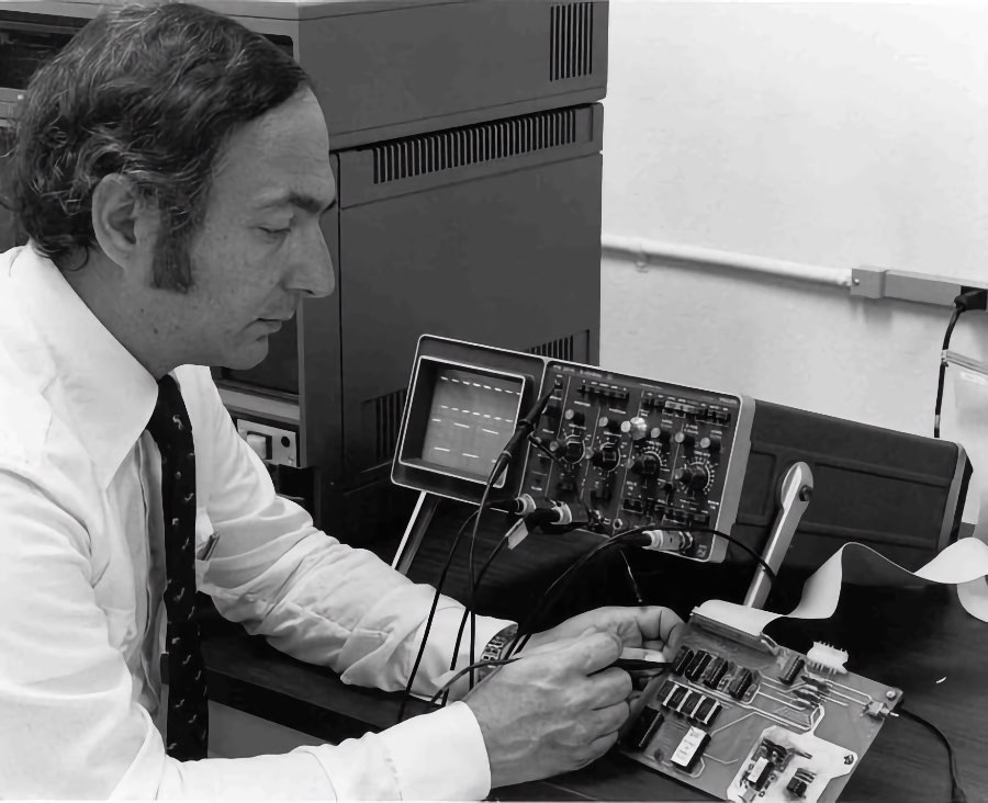
Faggin was granted Stan Mazor’s assistance, and the two engineers, based “in a very small office in Mountain View”, rolled up their sleeves. They took Hoff’s descriptions of the four Busicom chips’ functionality and architecture, refined them, did some fundamental preparatory work on how they might lay out the kind of circuits the chips would contain — all very different from the circuits found in Intel’s memory chips — and finally to turn them into the huge layout diagrams that could be photo-reduced to form the microscopic templates from which the chips’ circuits could be etched into silicon. Shima set to work on the code that the calculator’s processor would run.
Meanwhile, Hal Feeney continued to work on the CTC design. After three or four months, however, Intel bosses began to worry that CTC might not commission the 1201 after all: the customer did not now seem to be as committed to the project as it once was. Maybe it would be best to wait for a formal commission after all. So in July 1970 Feeney was reassigned to a memory chip project, and no further work was carried out on the 1201 until the end of the year. One reason for the concern that CTC might not require the 1201 was that it had been discovered that the VDU maker had also approached one of Intel’s more established rivals, Texas Instruments, an electronics and instrumentation company that had moved into integrated circuit design and manufacturing in the 1960s. Maybe CTC reached out to TI because wanted to ensure it would not be tied to a single supplier, or perhaps it hoped to double its chances of ending up with a working processor. It may even have been because Vic Poor’s brother Gus worked there. Whatever CTC’s reason, however, TI was eager to do the work, and the electronics giant put engineer Gary Boone on the case.

Intel’s work on the Busicom chip continued in the meantime. By October 1970 the Intel engineers had working prototypes of the chips that would be used in the Busicom calculator. The 4-bit 4004 CPU was accompanied by the 4001, a 256-byte read-only memory (Rom) chip which would hold the calculator-specific program safe from erasure; the 4002, 40-byte random access memory (Ram) chip to hold the sum being calculated and the answer; and the 4003, a 10-bit serial shift register chip to route input from the keypad and output to the calculator’s display to and from the 4004. All four chips, each connected up through 16 pins protruding from their ceramic casings, formed a single platform which Intel eventually called the MCS-4, short for Micro Computer System 4-bit. The 4001 came out of the factory in October 1970 and worked perfectly; so did the 4003, the following month. The 4002, also punched out in November 1970, showed a minor error but one that was soon fixed. The 4004, however, hadn’t been manufactured correctly, but when it was, in January 1971, it revealed some minor design issues that Faggin quickly put right. After further tests and design revisions, and the arrival of the calculator’s operating program from Busicom, Intel was finally able to confirm that Ted Hoff’s concept was right and that it worked. So did Busicom’s calculator. Intel put the 4000-series chips into production. That took place in February 1971; the following month, Intel shipped the first batch to Busicom for verification. In less than a year, what Hoff had conceived, Faggin had made a reality.
A new customer for the 1201
And, having finished the 4000 series designs, Faggin was immediately told to oversee the completion of the 1201. CTC may have gone cold, but Japan’s Seiko had come onto the scene to express a strong interest in an 8-bit processor for — guess what — a scientific calculator. Intel felt it had good reason to revive the project, whatever CTC was up to. Feeney was brought back to work alongside Faggin, who was also keeping an eye on the progress of the 4004 and its siblings. In the Summer of 1971, Faggin travelled to Europe to give a series of promotional talks on the capabilities and uses of the 4004. Back in Silicon Valley, Feeney continued to work on the 1201. The design work was done by the end of the year.
“Basically, I transferred my experience to Hal and then Hal pretty much went on his own,” said Faggin many years later. “Occasionally he needed some help in some issues, but fundamentally, Hal did the entire design by himself.”

Why was Faggin trying to help sell the 4004 to other potential customers? Surely it was a Busicom product? Back in the Spring, the relationship between Intel and the calculator company had changed. Yes, the MCS-4 was just what Busicom had ordered, but in the period since the company had made its initial approach to Intel — two years previously, don’t forget — the highly competitive Japanese calculator market had moved on: prices were plunging and buyers were demanding more functionality for their money. The same thing was happening in calculator markets across the Western world. Busicom was now concerned that the sum of money it had originally agreed to pay Intel for the chips would render the new device, even with four key components instead of ten, uncompetitive. At the same time, Faggin, now thoroughly convinced that the microprocessor was the key to Intel’s future success, nagged Intel co-founder Robert Noyce to reduce Busicom’s design fee in exchange for the right to offer the processor to other firms, though presumably not Busicom’s direct competitors. Hoff sided with Faggin, and that helped sway Noyce. However the deal came about, it involved waiving the $60,000 fee Busicom owed Intel — to the joy of Shima and his bosses. In return, the 400x family’s design, which ordinarily would have become the property of the client, was Intel’s to bring to market as it wished. Hence Faggin’s European tour the following Summer. Then, in November 1971, Intel went public with the 4004, advertising its “micro-programmable computer on a chip” to all comers.
CTC cuts Intel
Unfortunately for Intel, it wasn’t the only silicon chip maker attempting to integrate the functionality of a minicomputer processor board into a single chip. Over at Texas Instruments, engineer Gary Boone, working with Michael Cochran, was developing a very similar device. TI announced it to the world in June 1971, presenting a photo of its “CPU on a chip” in an Electronics magazine feature that claimed the new component would form the basis for an upcoming product from CTC. TI appeared to have beaten Intel to the punch.
At some point in 1971, CTC decided it no longer needed the Intel 1201. Undoubtedly, TI’s “CPU on a chip” announcement made it plain to Intel that its own design was not going to be commissioned by CTC after all. It certainly put the wind up Faggin and his colleagues until, working from the picture in the magazine article, they calculated the TI chip’s size at 215 x 225mm — 225 per cent bigger than the Intel 1201. Bigger meant more complex, and thus more costly to produce: the more complicated a chip’s circuitry, the more likely it is to be a dud when it comes out of manufacturing. Additionally, TI was rumoured to be experiencing problems turning its design into a product it could manufacture. Possibly this, but no doubt too a dramatic fall in the price of the rudimentary TTL ICs that CTC originally had thought to use, eventually persuaded the terminal maker that it didn’t want either TI’s chip or Intel’s. Federico Faggin maintains the TI chip never actually worked in any case. The latter was now formally rejected, and in the manner of the deal it had struck in the Spring with Busicom, Intel offered to waive CTC’s cancellation fee in return for the right to market the 1201 design in any way it saw fit.
The question of whether Intel or Texas Instruments invented the microprocessor chip has never been emphatically resolved, but the consensus now is that Intel got there first; TI’s first production microprocessor, the TMS1000, didn’t come to market until 1974, long after the 4004 and the 8008, the Intel-branded form of the 1201, had gone on sale. The second Intel microprocessor was released in April 1972. In any case, work would have begun on the proposed Busicom device first. However, TI was the first to file a patent, on Boone’s behalf, and since it detailed a processing system implemented on a single silicon chip — a “Computing System CPU”, in the words of US patent 3,757,306 — it covered enough of the 4004, 8008 and later designs to ensure that Intel was paying Texas Instruments royalties almost as soon as the patent was granted, in September 1973. With the patent came ‘ownership’ of the microprocessor right back to 1971 when the patent application was filed. Intel had the last laugh: it, not its competitor, has gone down in history as the inventor of the microprocessor. More to the point, Intel went on to become the world’s biggest chip company, on the back not of the memory chips it was founded to produce but the microprocessor. Intel subsequently patented work done on the 8080, the follow-up to the 8008, as a “Single-chip CPU”: number 4,010,449 with Faggin, Shima and Mazor the named parties. Gilbert Hyatt’s infamous “Single-chip integrated circuit computer architecture” filing is a whole other story…

At Intel, work on the 1201 continued after its rejection by CTC. Toward the end of 1971, Faggin uncovered a glitch that was causing test chips to fail intermittently. He furiously worked on a solution, found and implemented it. The chip maker was eventually able to schedule the 8008’s launch for April 1972. Once again, Intel offered the processor with as part of a platform, this time called MCS-8. Some existing Intel memory, storage and IO chips were selected and renamed, and they became the 8008’s companion chips.
Beyond the 8008
Neither the 4004 nor the 8008 set the market alight. Early applications included an elevator controller and a fuel station sales totaliser. “The wildest one I remember was that somebody supposedly put microprocessors on cows,” said Hoff in 2006. “The idea was to record when the cow went to the salt lick and when the cow went to the drinking stand. And so to get an idea of how much salt they consumed and how much water, and then to correlate that with milk production.” As Faggin later put it, those chips suggested there might be a market for microprocessors, but it was their successor, the 8080, which actually made it. Yes, they were general-purpose processors, but they had been nonetheless designed to sit inside specific products. The 8080 would be the first processor designed from the start with no specific application in mind: that would be left to the customer and the user to decide by way of the software they chose to run on the new chip.
Faggin badgered Intel chiefs to allow him to design the company’s third microprocessor before the 8008 had even been launched. His European tour in the Summer of 1971 had given users and potential customers an opportunity to point out their criticisms of the 4004’s design, and Faggin took these on board as he began to think through how be might design his next processor chip. But when he requested permission to develop it, early in 1972, he was instructed to wait: the company wanted to see how well the 4004 and the soon-to-be-launched 8008 would sell before it committed itself to a successor product. It wasn’t until the following Summer was past that Faggin was given the go-ahead. Like the 8008, the 8080 was an 8-bit processor, but it was much more complex and its design took much longer: Faggin, now joined by Masatoshi Shima, poached from Busicom, spent more than a year on the design and layout process. The first 8080s were punched out in December 1973. Minor errors fixed, a second, this time successful run of 8080s came off the production line in March 1974. Intel launched it the following month — the first true general-purpose microprocessor had arrived.
The 8080 really created the microprocessor market. The 4004 and 8008 suggested it, but the 8080 made it real — Federico Faggin
The 8080 went on to become the foundation of almost every mainstream processor Intel has made since, right up to the present day. They all use the same selection of core commands, the same instruction set, now called ‘x86’, from the 8086, the 8-bit 8080’s 16-bit successor. Different microprocessors have different instruction sets, though there is a great deal of commonality among the processes their respective instruction sets trigger. Some processor manufacturers use the same instruction set as competitors’ chips, to ensure compatibility between the two product lines. An example is the way microprocessors from chip maker AMD are today compatible with Intel processors because they too use the x86 instruction set. Federico Faggin left Intel late in 1974 to found Zilog, a company dedicated to microprocessor design — Intel had yet to stop making memory, as it later did. There he created the Z80, a chip which intentionally used the 8080 instruction set, though extended and expanded it, in order to take advantage of the mass of software that was beginning to accrete around the new Intel chip.

Not all chip makers took that path, though almost all of them began work on microprocessors of their own following the release of the 4004 and the 8008. Motorola released its 8-bit 6800 in March 1974, just ahead of the 8080. The 6800 was modelled on the architecture and instruction set of the processor used in DEC’s hugely popular PDP-11 minicomputer — just as Ted Hoff had done when considered the chip that would become the 4004. National Semiconductor’s 8-bit SC/MP debuted early in 1974 too. MOS Technology announced the 6501 and 6502 the following year. The 6501, which had been designed by a number of engineers who had worked on the 6800, was intended to be a plug-in replacement for the Motorola chip — in other words, a hardware manufacturer could switch from being a Motorola customer to an MOS one without having to alter their product. Motorola swiftly sued MOS. The 6502 had sufficient, though minor, differences to the 6501 so was safe from the Motorola legal team. It went on sale in September 1975. Federico Faggin’s Z80 debuted the following Spring.
That was in the mid-1970s. Within a couple of years, on both sides of the Atlantic, enthusiasts were becoming entrepreneurs and offering their designs as commercial systems, first as single-board computers — naked but complete circuit boards — then as packaged computers with integrated keyboards. Then came the killer applications, then the graphical user interface (GUI), then the OS wars — Windows vs Mac OS. By the 1990s, all personal computing was done on microprocessor-based systems. Many of PCs in use in business were linked over networks to microprocessor-based servers. Out went the minicomputer. The servers were soon connected to other servers, and data centers ditched mainframes for racks of microprocessor-filled units. Today, the entire Internet runs off them, as do the routers that manage the massive flow of data around the global network. Mainframes and minis are literally museum pieces.
Today there are billions, possible trillions, of microprocessors in use all over the world, in almost every electronic device. The Microprocessor has achieved this is its first 50 years. What will the next 50 years hold for this truly revolutionary technology?

CTC/Datapoint deserves more credit than you accord.
Inside the company the reason given for abandoning the 8008 was that it completely failed to implement Datapoint 2200 IO instructions. Faggin continued to be influenced by Datapoint architecture in his Z-80 design. The Z-80 added to an enhanced 8080 hardware for alternate registers, intended to speed subroutine calls, which was an innovation first implemented in the Datapoint 5500, successor to the 2200. Datapoint went on to use the Z-80 in a separate product line, the Datapoint 1500 series. There were enough differences between the 5500 and the Z-80 that code could not be directly used between them but with a micro library Datapoint’s assembler, SNAP-3, could be used in porting 5500 code over to the 1500’s Z-80. There were also some significant implementation differences between the 5500 hardware and the 1500’s architecture but they were primarily RAM memory addressing and IO related.
Datapoint was also first with local area networks, claiming that Datapoint customers already had 30,000 ARC systems deployed before Xerox delivered their first Ethernet node. Datapoint made many other significant innovations, some of them software. Datapoint’s Integrated Electronic Office System (IEOS) anticipated Microsoft’s by about a decade and included email, word processing, color business graphics (with color xerographic printers), video conferencing, and incorporated both wide area and local area networks. They were years ahead of the market.
One version of Datapoint’s story is written in
Datapoint: The Lost Story of the Texans Who Invented the Personal Computer Revolution
Datapoint’s demise was brought about not by technical failure but by Wall Street pandering (trying to maintain a 30% annual expansion, for example) and greed. It’s quite a story.